《Update:やっぱり A7 はサムスン製》
[iPhone 5S Teardown Round Up | YouTube]
世界でいの一番に iPhone 5S をバラシた iFixit・・・
iFixit: “iPhone 5s Teardown“: 20 September 2013
* * *

[ロジックボードの裏面]
Step 15:ロジックボードの裏面
ロジックボードの裏側に注目しよう。
Turning our attention to the backside of the logic board:
・プロセッサ[赤色]は Apple の A7 APL0698 SoC(MacRumors の投稿によれば、F8164A1PD という表示は 1GB の RAM を示すもののようだ)
– Apple A7 APL0698 SoC (based on this MacRumors post, the markings F8164A1PD indicate the RAM is likely 1GB)
・モデム[だいだい色]は Qualcomm の MDM9615M LTE
– Qualcomm MDM9615M LTE Modem
・トランシーバー[黄色]は Qualcomm の WTR1605L LTE/HSPA+/CDMA2K/TDSCDMA/EDGE/GPS
– Qualcomm WTR1605L LTE/HSPA+/CDMA2K/TDSCDMA/EDGE/GPS transceiver.
* * *
M7 コプロセッサは?
ウワサの M7 コプロセッサを探したが、どうやらそれは別個の IC かあるいは A7 に追加的に組み込まれた機能ではないかと思うようになった。
As we search for a much-anticipated M7 coprocessor, we begin to wonder if it actually is a separate IC, or if it is additional functionality built into the A7.
M7 の “M” は「マジカル」の “M” かもしれない。目にも見えず、その2つのデバイスをくっつけるのに妖精の魔法の粉を使っているのかもしれない。それとも “M” は「マーケティング」の意味か・・・
Maybe the “M” stands for “magical,” the M7 is invisible, and Apple does use pixie dust to hold the device together. Or perhaps the “M” stands for “marketing”…
アップデート:M7 が見つかった![注:《Update》参照]
Update: the M7 has been found!
* * *
製造日
われわれの機種に搭載された A7 は7月製造になっている。
Our A7 was fabbed in July.
* * *

[A7 プロセッサ]
Step 16:A7 プロセッサ
次はいよいよ新顔を調べる番だ。A7 は最高にクールだ。指紋センサーと併せて A7 のおかげで、消費者は 5C より 5S を選ぶ気にさせられる。
It’s time to investigate the new kid on the block, and it’s fly like an A7. Along with the fingerprint sensor, the A7 is a major enticement for consumers to pick the 5s over the 5c.
* * *
倍のパフォーマンス
広告によれば A7 プロセッサのパフォーマンスは 5(あるいは 5C)の A6 プロセッサの倍だという。
The A7 is advertised as providing twice the performance of the 5 (and 5c)’s A6 processor.
A7 に変えたことはスマートフォンとしては初めて 64-bit プロセッサを採用したことを意味する。AnandTech のレビューによれば、A7 のパフォーマンスが増えたその大部分は 64-bit アーキテクチャによるものではなく、古くなった ARMv7 命令セットに代えて新しくデザインし直された ARMv8 を採用したことによるもののようだという。
The switch to the A7 marks the first use of a 64-bit processor in a smartphone. Based on AnandTech’s review, it seems that the bulk of the A7’s performance gains do not come from any advantages inherent to a 64-bit architecture, but rather from the switch from the outdated ARMv7 instruction set to the newly-designed ARMv8.
新しい ARMv8 命令セットは 64-bit アーキテクチャを前提にデザインされている。過去20年にわたるレガシーのサポートを止めたことで効率が向上し、バッテリー持続時間を損なうことなくパフォーマンスを向上させた。
The modern ARMv8 instruction set was designed for a 64-bit architecture. It does away with the legacy support of the last 20 years, which increases efficiency, improving performance without sacrificing battery life.
* * *
チップメーカーは不明
このチップのメーカーが誰かはチップの内部を見るまでは分からない。[注:《Update》参照]
We’ll have to wait until we get inside the chip to find out who manufactured it.
* * *
新しい iPhone 5S の心臓部 A7 チップを製造したメーカーはいったい誰か・・・
★ →[原文を見る:Original Text]
❖ ❖ ❖
❖ ❖ ❖
《Update》やっぱり A7 はサムスン製(9月21日)
iFixit の iPhone 5S 分解は現在も進行中だが、新たに A7 プロセッサがサムスン製であることが分かった。
iFixit: “Apple’s A7 Processor is Made by Samsung” by Miro: 20 September 2013
* * *
A7 プロセッサはサムスン製
アップルの新しい A7 プロセッサのメーカーが誰なのかインターネットではさまざまな憶測がなされた。昨夜われわれは iPhone 5S を分解したが、Chipworks がさらに一歩進めた。IC デキャッピングの結果、その内部写真から A7 がサムスン製であることが分かった。
There was mighty speculation among the internet as to the manufacturer of Apple’s new A7 processor. We uncovered it last night during the iPhone 5s teardown, but now Chipworks has taken it one step further. Through the magic of decapping an IC, their internal shots revealed the A7 to be made by Samsung.
* * *
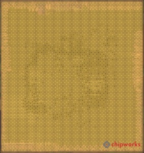
[A7 ダイ写真:Chipworks 提供]
サムスンの HKMG を使用
Chipworks によれば、「まず初期の分析として、A7 がサムスンの半導体ファウンドリで製造されたことを確認した。さらに分析を進めれば、本日中にはプロセスタイプおよびノードも確認できるだろう。それはそれとして、サムスン 28 nm Hi K metal Gate (HKMG)が使用されているものと考えられる。同様の工程はサムスンの Galaxy S IV で用いられている Exynos Application プロセッサでも確認されている。その点が確認され次第、あるいはそれとは異なる情報が得られ次第、われわれのエンジニアはアップルの A7 を解体処理することになる。
From Chipworks: “We have confirmed through early analysis that the device is fabricated at Samsung’s Foundry and we will confirm process type and node later today as analysis continues. That being said, we suspect we will see Samsungs 28 nm Hi K metal Gate (HKMG) being used. We have observed this same process in the Samsung Exynos Application processor used in the Galaxy S IV. Our engineers will be deprocessing the Apple A7 as soon as they can to confirm this or to provide different information.”
* * *
さらに分解の第一段階では分からなかった M7 プロセッサの正体も分かった。
iFixit: “Apple’s Mysterious M7 Processor Uncovered” by Miro: 20 September 2013
* * *

[見つかった NXP プロセッサ:Chipworks 提供]
M7 プロセッサの正体
Chipworks がさらに詳しく調べたところ、アップルのミステリアスな M7 プロセッサの正体が分かった。昨夜の iPhone 5S 分解ではどうしても分からなかったものだ。それは NXP 製の LPC1800 で、ネオプレンのようなカバーの下に隠れていた。
Further digging by Chipworks gave us the identity of Apple’s mysterious M7 processor, a chip that was conspicuously absent from last night’s iPhone 5s teardown. It’s an NXP LPC1800 device that was buried beneath a neoprene-looking cover:
* * *
センサーからのインプット解析・処理専用
Chipworksによれば、「M7 はプリント基板に実装されたジャイロスコープ、加速度計、電磁コンパスなどの個別のセンサーからのインプットを処理、解析する専用プロセッサだ。これらのセンサーは、アップルのこれまでのやり方からみて、加速時計及びジャイロスコープは STMicroelectronics 製、電磁コンパスは旭化成マイクロデバイス(AKM)製だろうと考えられる。その後コンパスは AKM の AK8963 であることが確認された。」
From Chipworks: “The M7 is dedicated to processing and translating the inputs provided to it by the discrete sensors; the gyroscope, accelerometer and electro magnetic compass mounted throughout the main printed circuit board. Traditional Apple techniques lead us to believe that the these discrete sensors will most likely be STMicroelectronics for the accelerometer and the gyroscope while the electro magnetic compass would again be an Asahi Kasei Microdevices (AKM). We have since confirmed the compass to be AKM’s AK8963.”
* * *
実機さえ入手できれば、たった2日でここまで分かるんだ!
A7 がサムスン製なら、サムスンだってすぐに 64-bit 対応できるということか?
そういえば、iPhone 5S 発表直後にサムスンが次期 Galaxy は 64-bit プロセッサを搭載する[こちらも]といったのはこういうことだったのか・・・
★ →[原文を見る:A7 Processor]
★ →[原文を見る:M7 Coprocessor]

コメントを残す